The boards are assembled, starting with one of the easy ones. The process is easy, clean the board and its stencil with Isopropyl Alcohol (IPA), then place the stencil on top of the board, using other boards to hold everything level, tape it down to stop it moving, then using an old plastic store card, apply solder paste to all of the board, cleaning off any excess as you go. You don't really use much solder paste at all, since the area is very small and the stencils are quite thin (0.12mm thick).
Now to remove the stencil, without moving it on the freshly pasted board, as that means you have to clean the board and start again, wasting the solder paste. Once the stencil is off, it needs a clean up to remove the solder paste, this is done with some IPA. Now you just need a high temperature mat on the desk (forward planning for soldering) the bill of materials and the components ready, apply them down one by one using some long needle nose tweezers and a little pressure to make them stick to the solder paste, so they don't fall off when you are doing the subsequent components.
You don't need to worry too much about exact placement on the chips as the surface tension of the solder will pull them into place when you apply heat. Soldering is simply the application of hot air to the board, not to the components, using the hot air soldering station, a little nudge here and there with the tweezers to make things line up properly, and you are done. Once the board has cooled, its time to apply all the through-hole components such as connectors, headers and pins to all the diagnostic pins (I2C, SPI, etc). Once that is all done, time for another clean up with IPA to remove any flux and make everything look nice and clean.
Front Panel
This is the assembled front panel. the TFT, still with its protective film in place (notice the tab colour, we'll come back to that later). The TFT drops on top, using the 4 mounting posts and some long pin strips, into the connectors on the PCB.
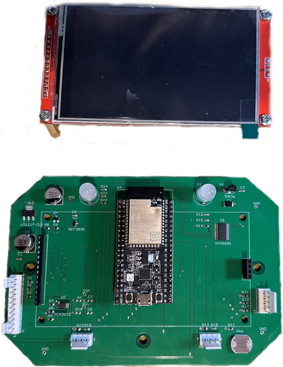
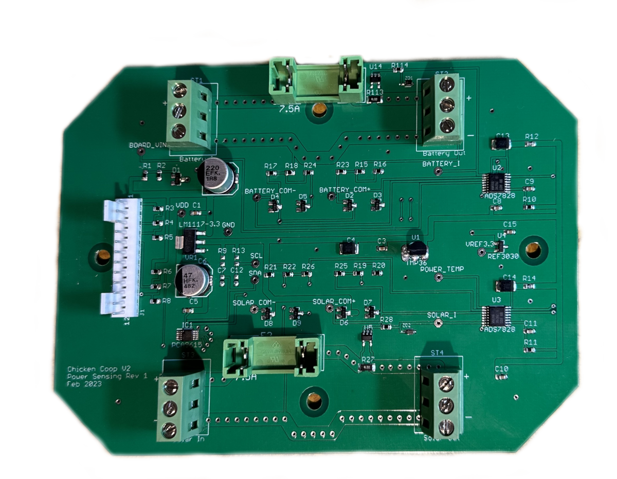
Power Sensing
The power sensing board is the next easiest one to do, so that came up next, its the same assembly process, just with a few more components to apply.
The main board
The last board to assemble is the main board, this is an order of magnitude more difficult to assemble, since its got a lot more components and being a lot larger, actually getting to where you need to be, without touching the solder paste across the whole board is much more challenging, you end up using two hands, one to support the other, to give yourself the additional reach you need to get to the other components.
There are a number of small decoupling capacitors on the back of the board, in general, these are directly under the IC's on top, since that is best practice, since its the shortest distance from the capacitor to the power pins on the IC and therefore the best for providing instantaneous power during switching within the IC. These must be applied and soldered into place first, then, when heating the top of the board later on, no movement can occur, otherwise those capacitors will come off again.
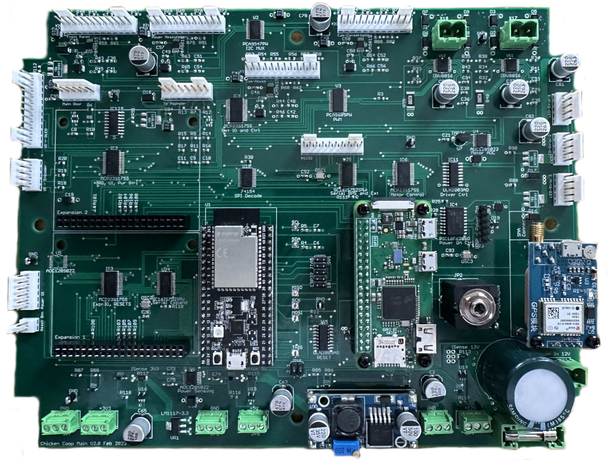
This picture shows the various modules fitted in their normal positions, although all of them were removed before powering up. Bottom right is a small ready-made regulator board, this was used in preference to a linear module, since it is more power efficient and produces a lot less heat, it can also be set to produce the correct output voltage before applying it to the board, so that nothing nasty happens to the IC's on the board. This was simpler and lower risk than manufacturing it onto the board directly. A large green capacitor can be seen in the bottom right, this is the local power reserve, since all the boards power comes in via the connector and fuse adjacent to it.
Once all of these boards were produced, a second set of each was assembled, this gives two, theoretically identical boards, so if you are chasing a problem later, you can swap boards to help rule out any assembly problems or bad components.